Halbleiter - Lumineszenzscanner
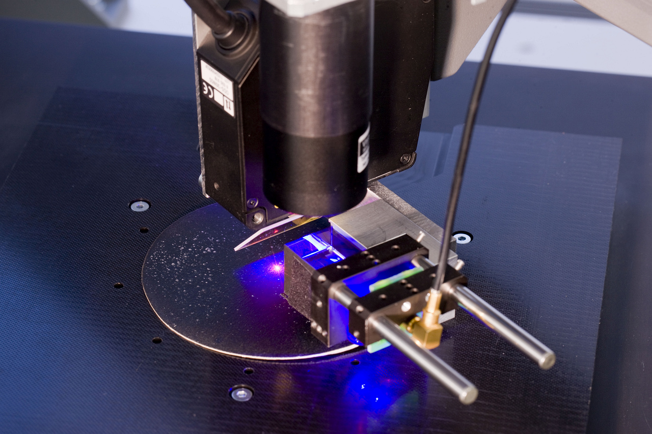
Photoluminescence Scanner (SiC Wafer)
We are very pleased to announce that our activity for a photoluminescence scanner was awarded the Semikron Innovation Award 2016 at the power electronics conference PCIM in Nuremberg. The official press release can be found here.
Raise the efficiency of your production
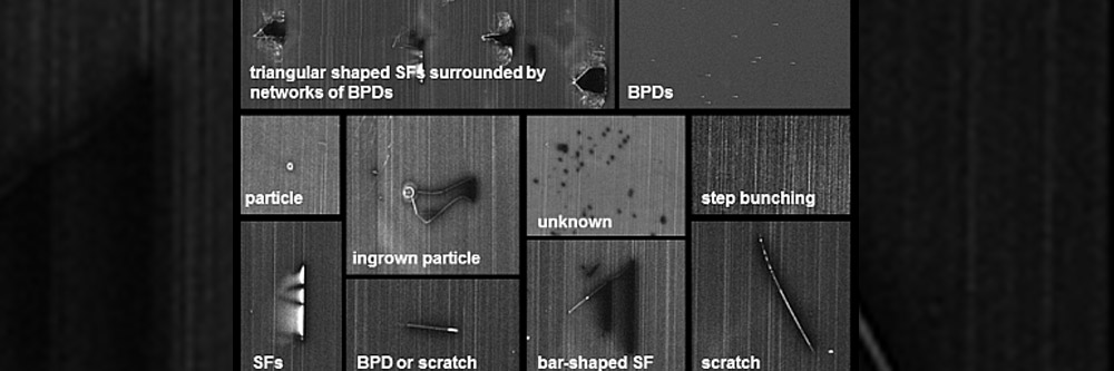
In the last decade, the interest in silicon carbide (SiC) high power application devices has grown significantly due to the positive properties of SiC. Despite great improvements in the material quality of 4H-SiC substrates and epiwafers within the last years, critical crystallographic defects such as stacking faults (SFs) and basal plane dislocations (BPDs) can still lead to bipolar degradation and finally the complete failure of the device.
In this context, Intego developed a new photoluminescence scanner in 2016 in collaboration with the Fraunhofer institute IISB and other partners from industry and academia. We concentrate on the inspection of SiC wafers.
The scanner provides short inspection times that are suitable for an industrial application. The previous techniques are either destructive (selective etching) or very cost-intensive (synchrotron X-ray radiation).
Performance data
The new developed photoluminescence scanner for SiC wafers achieves reliable identification of the most significant crystallographic defects. In the scanning process, a specific UV laser is used as the excitation source (wavelength 325 nm) in combination with a sensitive EMCCD camera.
- The depth of the beam penetration is 7 µm. This allows the identification of crystallographic defects near the surface or of those located in deeper layers.
- The lateral resolution is 5 µm.
Our system detects the following defects.
- Stacking faults (SFs)
- Basal plane dislocations (BPDs)
- Threading dislocations (TDs)
Further options
If you require an individual solution, Intego offers free-of-charge feasibility studies based on sample parts. The prepared study will include a system design with draft specifications and a price estimate. Do not hesitate to contact us directly.
A further report about our inspection system was published in the EEtimes.
The scientific paper containing more details about the SiC inspection can be downloaded here.
PCO wrote an application report here.
Your contact for photoluminescence scanner

Dr. Steffen Oppel
+49 9131 61082-230
steffen.oppel@intego.de